One of the most challenging tasks in PCB prototyping is the design and layout of the circuit diagram, as it directly affects the performance and stability of the electronic product. A well-designed and laid-out circuit diagram can improve product reliability and reduce the possibility of problems, while a poor circuit diagram can cause the electronic product to malfunction or damage its components.

When designing a circuit diagram for PCB prototyping, it is necessary to consider the power and signal integrity of the circuit. In terms of power, the power requirements of each component must be determined to select suitable components and power sources. In terms of signal integrity, attention must be paid to impedance matching, signal transmission line length and direction, to minimize signal distortion and reflection. In addition, electromagnetic compatibility (EMC) issues must also be considered to ensure that the circuit board does not interfere with or be interfered by other devices.
In addition to these factors, attention to detail is also a crucial part of the circuit diagram design and layout for PCB prototyping. For example, wire lengths should be kept as short as possible to reduce signal transmission delay and power loss. Components should be arranged reasonably to avoid interference between them. Impedance matching is also critical and should be done to avoid impedance mismatch, which can reduce signal distortion and reflection.
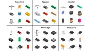
When dealing with signals, it is important to separate the signal ground from the power ground and use appropriate connection methods to reduce ground loop feedback and interference. In addition, when laying out the circuit board, care must be taken to avoid mutual interference between components such as transistors, inductors, and capacitors, to reduce noise and interference.
To design and layout the circuit diagram, professional software such as Altium Designer and Eagle PCB is needed to accomplish this task. These software provide various tools and resources to help engineers design and layout the circuit diagram more effectively. Moreover, simulators and emulators should be used to verify the circuit’s performance and stability, ensuring the quality and reliability of the electronic product.
In conclusion, designing and laying out the circuit diagram is one of the most important and challenging steps in the PCB prototyping process. When designing and laying out the circuit diagram, various factors such as power, signal integrity, and EMC must be considered to ensure the quality and reliability of the electronic product. Attention to detail is also crucial to reduce problems such as signal distortion, reflection, and noise interference.
Talk To A Startsmall Technology PCB’A Expert Now!
We look forward to working with you side by side, to be a long-term partner whom you can trust.


