How Does a Full Turnkey PCB Assembly Work?
Your trusted partner of PCB manufacturing & Assembly
Step 1: Communication
 
															1.If you haven’t created your schematics or they need updating
let us know and we’ll work with you to make them perfect.
2.Already have ideal designs and need to get a quote
For a quick and good quotation, We need the following information:
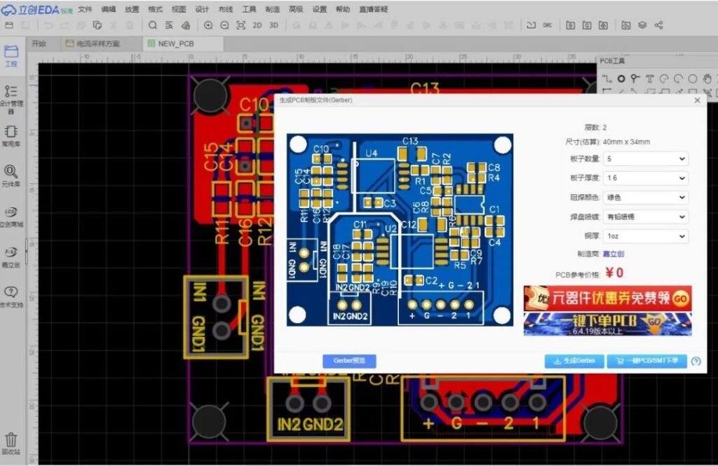
Gerber file (RS-274-X, or RS-274-D format), it should include following:
- Trace layer
- Aperature/D code file
- NC Excellon Drill File
- Drill Tool list (if not listed in NC Drill file)
- Soldermask
- Silkscreen
- Readme.txt file
We can also accept other file, such as .PCB, PCBDOC, BRD, CAM, CAD, ODB++(.tgz), ASC and DXF.
Quantity (prototype, volume production)
Lead time requirements
For PCBA, please also provide:
BOM (.xls, .xlsx)
Pick & place file (.xls, .xlsx, .txt, csv)
*Startsmall Tech promises not to disclose any design/manufacture files about your project. We can sign NDA with you to ensure the safety of your project.
Step 2: Review and Manufacturing
Upon prototype validation and customer approval, all PCBs will proceed to full-scale production with mandatory 100% visual inspection and E-testing. Comprehensive quality certification packages will be provided for technical review.
| Production | Layers | Normal Service | Expedited Service | 
|---|---|---|---|
| FR4 PCB | 1 Layer | 4-6 days | 2-3 days | 
| 2 Layers | 5-8 days | 2-3 days | |
| 4Layers | 8-12 days | 3-5 days | |
| 6 Layers | 8-12 days | 4-6 days | |
| 8 Layers | 12-16 days | 6-8 days | |
| 10 Layers | 18-20 days | TBD | |
| HDI(1+N+1,2+N+2) | 3-4 weeks | TBD | 
| Mass Production | Layers | Normal Service | Expedited Service | 
|---|---|---|---|
| Metal Core PCB | 1 Layer | 2 – 2.5 weeks | 1 week | 
| 2 Layers | 3 – 4 weeks | 1.5 – 2 weeks | |
| 4 Layers | 4 – 5 weeks | 2 weeks | |
| 6 Layers | 5 – 6 weeks | 2.5 weeks | |
| 8 Layers | 6 – 7 weeks | 3 – 4 weeks | |
| 10 Layers | 7 – 8 weeks | TBD | 
| Production | Layers | Normal Service | Expedited service | 
|---|---|---|---|
| Ceramic PCB | 1 Layer | Thick Film:3.5 – 4 weeks DCB/DBC/AMB: 4 – 5 weeks DPC: 4 – 5 weeks | Thick Film:1.5 – 2.5 weeks DCB/DBC/AMB: 2.5 – 3.5 weeks DPC: 2 – 3 weeks | 
| 2 Layers | Thick Film:4.5 – 5.5 weeks DCB/DBC/AMB: 5 – 6 weeks DPC: 5 – 6 weeks | Thick Film:2 – 3 weeks DCB/DBC/AMB: 3 – 4 weeks DPC: 2.5 – 3.5 weeks | |
| 4 Layers | Thick Film: 5 -6 weeks | 2.5 – 3 weeks | |
| 6 Layers | Thick Film: 5 -6 weeks | 3 – 3.5 weeks | |
| 8 Layers | Thick Film: 6 -7 weeks | 3 – 4 weeks | |
| 10 Layers | Thick Film: 7 – 9 weeks | 4 – 5 weeks | 
| Mass Production | Layers | Normal Service | Expedited Service | 
|---|---|---|---|
| Flexible PCB | 1 Layer | 1.5 – 2 weeks | 1 week | 
| 2 Layers | 2 – 2.5 weeks | 1 week | |
| 3 Layers | 2.5 – 3 weeks | 1.5 weeks | |
| 4 Layers | 3 – 4 weeks | 1.5 weeks | |
| 6 Layers | 4 – 5 weeks | 1.5 – 2 weeks | |
| 8 – 12 Layers | 5 – 7 weeks | 2 – 3 weeks | 
| Mass Production | Layers | Normal Service | Expedited Service | 
|---|---|---|---|
| Rigid-flex PCB | |||
| 2 Layers | 2.5 – 3.5 weeks | 1.5 weeks | |
| 3 Layers | 3 – 4 weeks | 2 weeks | |
| 4 Layers | 4 – 5 weeks | 2.5 weeks | |
| 6 Layers | 5 – 6 weeks | 3 weeks | |
| 8 – 12 Layers | 6 – 8 weeks | 3.5 weeks | 
 
															Step 3: Components Sourcing
 
															Our cross-functional procurement specialists leverage 18+ years of PCB component supply chain expertise to preemptively resolve sourcing challenges. Through comprehensive BOM validation and AVL management, we implement proactive risk mitigation strategies during project planning stages, ensuring zero component-related delays in your production cycles.
- Purchase from major and verified distributors
- Provide Alternative PN Plan to save cost
- Fully traceable by ERP and MES system
- Transparent and efficient platform
- Using alternative brand (↓10-30%)
- Re-design(≥30%)
Step 4: PCB Assembly
We are equipped with the state-of-the-art manufacturing facility and sophisticated machinery to support the fabrication. We also have highly trained and experienced personnel to make sure your project is done faster with high quality.
We offer consignment, full turnkey and partial turnkey assembly services.
We source all the parts directly from the manufacturers or from authorized distributors to avoid counterfeit parts.
Standard leads times range from 1-15 days. If BOM purchased by us, and the parts are not in stock,1 week will be added for most cases
 
															Step 5: PCBA Inspection and Testing
 
															We strictly follow the international standards and customer standards to inspect and control the delivery quality.
We have developed a fully controlled in-house quality test process to assure the quality of the products we deliver.
- First Article Inspection (FAI)
- Automatic Optic Inspection(AOI)
- X-Ray inspection
- Functional Test
- Final Quality Assurance (FQA)
Step 6: Packing & Shipping
Packaging usually involves sealing the material around the printed circuit board to keep dust, moisture and other foreign objects out. All our PCB boards are shipped in vacuum packages. All our PCBA boards are shipped with anti-static packaging and Shock-proof packaging.
You can choose among various shipping methods and have the products delivered at any destination all around the world. Follows are some Standard Shipping Times for your reference.
- DHL/UPS/Fedex: 2-6 working days
- TNT: 4-9 working days
- EMS: 8-15 working days
- By Air: 4-9 working days
- By Sea: 30-50 working days
 
															Step 7: After-sale Service
 
															Delivery is not the end,just the beginning of next cooperation.
We timely follow up the quality performance of the products after delivery, and take quick and effective improvement actions for the feedback of customer’s abnormal condition.
If there is any problem with your order, our team of engineers will conduct a meeting for a solution within 48 hours.
Talk To A STARTSMALL Technology PCBA Expert Now!
We look forward to working with you side by side, to be a long-term partner whom you can trust.
