
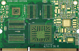
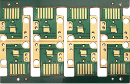
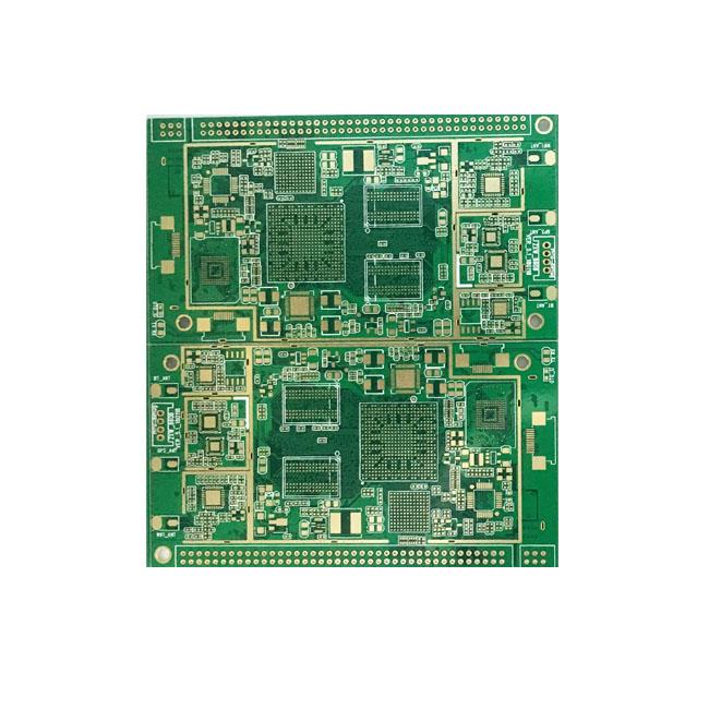
PCB Prototyping
- Can be expedited in eight hours,
- same-day orders, same-day shipments
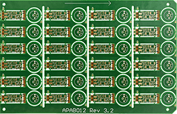
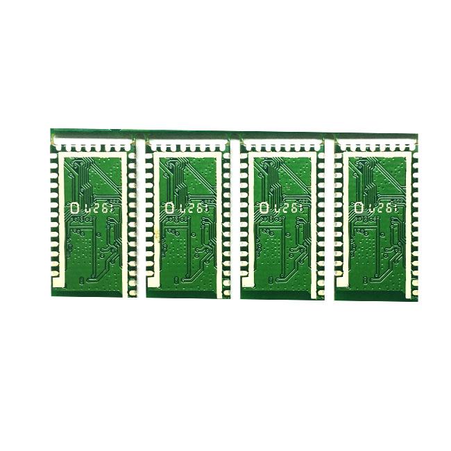
Low-Volume Fabrication
- The through rate is over 99%
- Delivery within 5 square meters in 3 days
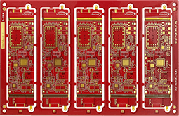
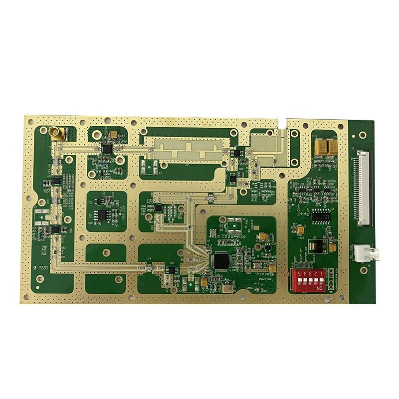
High Precision PCB
- Resistance welding bridge, through hole plug oil process, electrical gold finger, circuit precision and so on
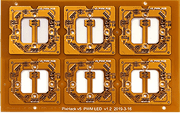
FPC Flexible Board
- The quality of raw materials, Taihong and other brands is guaranteed
- Soft and hard combination, FPC multilayer board, wiring, etc.
Copper Substrate
- Thermoelectric separation process, 100% computer open short circuit test, high heat dissipation performance, for the radiator, power supply, etc.
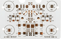
Aluminum Substrate
- Aluminum Plate + high thermal conductivity insulation material, high thermal conductivity, can do 8-layer mixed aluminum substrate
Our PCB Fabrication process


Rapid PCB Prototyping
If you are introducing a new product, PCB prototyping is the easiest and most cost-effective way to detect and fix errors. This method helps to reduce the risk of costly rework during mass production.
At our company, we provide a rapid prototype-making service, as well as reverse engineering for existing assemblies.
- Online Support 24/7
- 24 hours fast PCB prototype expedite services
- Free DFM & DFA Check
- No minimum order requirement
| Prototype(<1m²) | Layers | Normal Service | Expedited Service |
|---|---|---|---|
FR4 PCB | 1 Layer | 3 – 4 days | 24 hours |
2 Layers | 4 – 6 days | 24 hours | |
4 Layers | 8 -10 days | 48 hours | |
6 Layers | 8 – 10 days | 72 hours | |
8 Layers | 10~14 days | 72 – 96 hours | |
10 Layers | 14-18 days | 120 – 168 hours | |
HDI (1+N+1 2+N+2) | 2.5 – 3.5 weeks | TBD |
| Prototype(<1m²) | Layers | Normal Service | Expedited Service |
|---|---|---|---|
Metal Core PCB | 1 Layer | 1 – 1.5 weeks | 48 hours |
2 Layers | 2.5 – 3 weeks | 168 hours | |
4 Layers | 3 – 4 weeks | 1.5 weeks | |
6 Layers | 4 – 5 weeks | 2 weeks | |
8 Layers | 5 – 6 weeks | TBD | |
10 Layers | 6 – 7 weeks | TBD |
| Prototype(<1m²) | Layers | Normal Service | Expedited Service |
|---|---|---|---|
Ceramic PCB | 1 Layer | Thick Film:3 – 3.5weeks DCB/DBC/AMB: 3 – 4 weeks DPC: 2 – 3 weeks | Thick Film:1.5weeks DCB/DBC/AMB: 2 – 3 weeks DPC: 1.5 weeks |
2 Layers | Thick Film:3 – 4 weeks DCB/DBC/AMB: 3.5 – 4.5 weeks DPC: 2.5 – 3.5 weeks | Thick Film:2 weeks DCB/DBC/AMB: 2.5 – 3.5 weeks DPC: 2 weeks | |
4 Layers | Thick Film: 4 – 6 weeks | 2.5 weeks | |
6 Layers | Thick Film: 4.5 – 6 weeks | 2.5 weeks | |
8 Layers | Thick Film: 5 -7 weeks | 3 weeks | |
10 Layers | Thick Film: 6 – 8 weeks | 3.5 – 4 weeks |
| Prototype(<1m²) | Layers | Normal Service | Expedited Service |
|---|---|---|---|
Flexible PCB | 1 Layer | 0.5 – 1 week | 48 hours |
2 Layers | 0.5 – 1 week | 48 hours | |
3 Layers | 1.5 – 2 weeks | 72 hours | |
4 Layers | 2.5 – 3 weeks | 96 hours | |
6 Layers | 3 – 4 weeks | 120 hours | |
8 – 12 Layers | 4 – 5 weeks | 144 hours |
| Prototype(<1m²) | Layers | Normal Service | Expedited Service |
|---|---|---|---|
Rigid-flex PCB | |||
2 Layers | 1.5 – 2 weeks | 5 days | |
3 Layers | 2 – 2.5 weeks | 6 days | |
4 Layers | 2.5 – 3.5 weeks | 1 week | |
6 Layers | 3.5 – 4 weeks | 1.5 weeks | |
8 – 12 Layers | 4 – 5 weeks | 2 weeks |
Free DFM & DFA Check
Startsmall Tech offers free PCB file checks to ensure that there are no missing components or construction errors, and that the designs are compatible with our production process.
Our team of manufacturing experts can provide recommendations for cost optimization on your prototype designs.
Additionally, our prototypes are constructed according to the same ISO-9001-2015 and IPC quality standards used in production jobs, ensuring consistency even at large volumes.
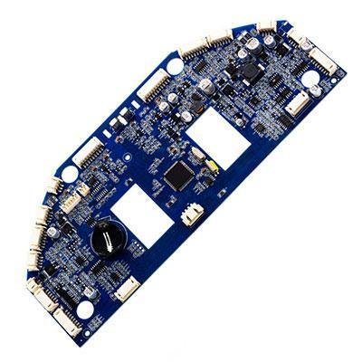
PCB Reverse Engineering
We also offer reverse engineering of existing assemblies.
We can take an existing board from a bare board, an assembled board, existing drawings, and we can create a new design with all supporting documentation.
PCB Prototype Capability
Follows are basic PCB production cabability, but we are not limited by that

Conventional PCB | |
| The conventional PCBs have electrical connection on the normal FR-4 material through the vias. After a long-term development, it has evolved from single-layer to double-layer, multi-layer PCBs. | |
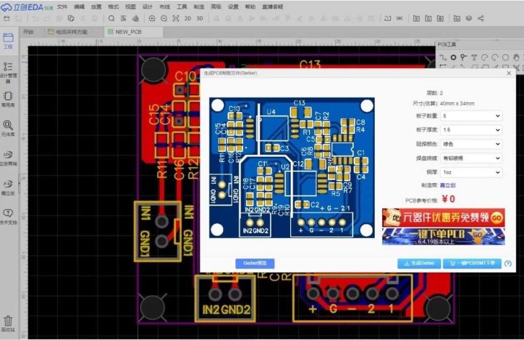
| PCB circuit board Files format: | Gerber, .pcb, .pcbdoc or .cam |
| Printed circuit board Materical: | FR4 |
| PCB board Surface Finishing: | ENIG/OSP/Gold Plating(Soft/hard) /HASL/Imm. Silver/IMM.Tin/Tin Plating/Carbon Ink/Selective /Imm.metal+OSP |
| PCB board Cooper Thickness: | 0.5OZ-12OZ |
| Printed circuit board Layer: | 1-24 Layer |
| Printed circuit board thickness: | 0.25mm -10mm |
| Min PCB Line Width/Spacing: | 0.075mm/0.065mm |
| PCB board Min S/M Bridge: | 0.075mm |
| Min PCB PTH Hole Size: | 0.15mm |
| Min PCB Microvia Hole Size: | 0.1mm |
| PCB board Outline Tolerance : | ±0.10mm |
| PCB PTH Aspect Ratio : | 10/0.1 |
| Impedance Control Single-ended/Differential: | ±10% |
| PCB board Bow and Twist : | 0.75% |
Sample PCB Producing Leadtime | ||
PCB layer | Urgent (hour) | Normal (day) |
1 、2L | 24 | 4–5 |
4L | 48 | 5–7 |
6 、8L | 72 | 7–9 |
10 L and up | To be determined based on gerber file | |
The above lead time is based on: | 1.Material Available | |
2.All Engineering issues comfirmed | ||
PCB Mass Producing Leadtime | ||
PCB layer | Urgent (hour) | Normal (day) |
1 、2L | 24 | 4–5 |
4L | 48 | 5–7 |
6 、8L | 72 | 7–9 |
10 L and up | To be determined based on gerber file | |
The above lead time is based on: | 1.Material Available | |
2.All Engineering issues comfirmed | ||

Flexible PCB | |
Flexible printed circuit boards (FPC) has become a common component of electronic products due to its lightness and flexibility performance. It is widely used in smart terminal, wearable electronics, consumer, automotive, industrial and medical fields. The miniaturization and integrated function of electronics product development is driving FPC to fine line and multilayer design. | |
PCB circuit board Files format: | Gerber, .pcb, .pcbdoc or .cam |
Printed circuit board Materical: | PI (polyimide), PET, electrolytic copper, calendered copper |
PCB board Surface Finishing: | OSP HASL, Lead-free HASL, Immersion gold, Hard gold, Immersion silver, OSP |
PCB board Cooper Thickness: | 12UM 18UM 36UM 70UM |
Printed circuit board Layer: | 1-14 Layer |
Printed circuit board thickness: | 0.06-0.4mm |
Min PCB Line Width/Spacing: | 0.045mm/0.045mm |
Insulating layer thickness: | 12.5um 25UM 50UM |
Min PCB PTH Hole Size: | 0.15mm |
Min PCB Microvia Hole Size: | 0.1mm |
Maximum PCB board size: | 250*4000mm |
Thickness tolerance of finished PCB : | ±0.03mm |
Impedance Tolerance: | 50Ω -120Ω |
PCB Stiffener : | FR4, PI, PET, SUS,PSA |
Sample PCB Producing Leadtime | ||
PCB layer | Urgent (hour) | Normal (day) |
1 、2L | 48 | 5–7 |
4L | 96 | 7–10 |
6 、8L | 144 | 12–16 |
10 L and up | To be determined based on gerber file | |
The above lead time is based on: | 1.Material Available | |
2.All Engineering issues comfirmed | ||
PCB Mass Producing Leadtime | ||
PCB layer | Urgent (hour) | Normal (day) |
1 、2L | 72 | 5–7 |
4L | 120 | 7–10 |
6 、8L | 168 | 12–16 |
10 L and up | To be determined based on gerber file | |
The above lead time is based on: | 1.Material Available | |
2.All Engineering issues comfirmed | ||


Rigid-Flex PCB | |
Rigid-Flex printed circuit boards are boards using a combination of flexible and rigid board technologies in an application. Most rigid flex boards consist of multiple layers of flexible circuit substrates attached to one or more rigid boards externally and/or internally, depending upon the design of the application. The flexible substrates are designed to be in a constant state of flex and are usually formed into the flexed curve during manufacturing or installation. | |
PCB circuit board Files format: | Gerber, .pcb, .pcbdoc or .cam |
Printed circuit board Materical: | PI (polyimide), PET, electrolytic copper, calendered copper,FR4 |
PCB board Surface Finishing: | OSP HASL, Lead-free HASL, Immersion gold, Hard gold, Immersion silver, OSP |
PCB board Cooper Thickness: | 12UM 18UM 36UM 70UM |
Printed circuit board Layer: | 2-14 Layer |
Printed circuit board thickness: | 0.25-6.0mm |
Min PCB Line Width/Spacing: | 0.045mm/0.045mm |
Insulating layer thickness: | 12.5um 25UM 50UM |
Min PCB PTH Hole Size: | 0.15mm |
Min PCB Microvia Hole Size: | 0.1mm |
Maximum PCB board size: | 250*4000mm |
Thickness tolerance of finished PCB : | ±0.03mm |
Impedance Tolerance: | 50Ω -120Ω |
PCB Stiffener : | FR4, PI, PET, SUS,PSA |
Sample PCB Producing Leadtime | ||
PCB layer | Urgent (hour) | Normal (day) |
1 、2L | 48 | 5–7 |
4L | 96 | 7–10 |
6 、8L | 144 | 12–16 |
10 L and up | To be determined based on gerber file | |
The above lead time is based on: | 1.Material Available | |
2.All Engineering issues comfirmed | ||
PCB Mass Producing Leadtime | ||
PCB layer | Urgent (hour) | Normal (day) |
1 、2L | 72 | 5–7 |
4L | 120 | 7–10 |
6 、8L | 168 | 12–16 |
10 L and up | To be determined based on gerber file | |
The above lead time is based on: | 1.Material Available | |
| 2.All Engineering issues comfirmed | |
Rogers PCB | |
Attributes details | |
PCB circuit board Files format: | Gerber, .pcb, .pcbdoc or .cam |
Printed circuit board Materical: | Rogers 4350B, Rogers 3003,Rogers 3006,Rogers 3010,Rogers 0588,Rogers 6002,Rogers 6010,Rogers 4003,Rogers 4835,Rogers 4360G2 |
PCB board Surface Finishing: | ENIG/OSP/Gold Plating(Soft/hard) /HASL/Imm. Silver/IMM.Tin/Tin Plating/Carbon Ink/Selective /Imm.metal+OSP |
PCB board Cooper Thickness: | 0.5OZ-12OZ |
Printed circuit board Layer: | 1-24 Layer |
Printed circuit board thickness: | 0.25mm -10mm |
Min PCB Line Width/Spacing: | 0.075mm/0.065mm |
PCB board Min S/M Bridge: | 0.075mm |
Min PCB PTH Hole Size: | 0.15mm |
Min PCB Microvia Hole Size: | 0.1mm |
PCB board Outline Tolerance : | ±0.10mm |
PCB PTH Aspect Ratio : | 10/0.1 |
Impedance Control Single-ended/Differential: | ±10% |
PCB board Bow and Twist : | 0.75% |
Sample PCB Producing Leadtime | ||
PCB layer | Urgent (hour) | Normal (day) |
1 、2L | 24 | 4–5 |
4L | 48 | 5–7 |
6 、8L | 72 | 7–9 |
10 L and up | To be determined based on gerber file | |
The above lead time is based on: | 1.Material Available | |
2.All Engineering issues comfirmed | ||
PCB Mass Producing Leadtime | ||
PCB layer | Urgent (hour) | Normal (day) |
1 、2L | 24 | 4–5 |
4L | 48 | 5–7 |
6 、8L | 72 | 7–9 |
10 L and up | To be determined based on gerber file | |
The above lead time is based on: | 1.Material Available | |
| 2.All Engineering issues comfirmed | |

High Tg PCB | |
The Glass Transition Temperature (Tg) is one of the most important properties of any epoxy and is the temperature region where the polymer transitions from hard, glassy material to a soft, rubbery material. Circuit board material must flame-resistant, it can’t be burned at a certain temperature and only be softened. The temperature point is called the glass transition temperature (Tg). The higher Tg point means a higher temperature requirement during lamination. And the boards will be hard and crisp, which will affect the hole and the electrical properties. Ordinary PCB materials at high temperatures, not only will be softened, deformation, melting and other phenomena, but also the mechanical and electrical properties decline sharply. General FR4 Tg is 130-140 centigrade, moderate Tg is greater than 150-160 centigrade, High-Tg is greater than 170 degrees. The higher of Tg, the better the performance of PCB heat resistance, moisture resistance, chemical resistance, stability and other characteristics. | |
PCB circuit board Files format: | Gerber, .pcb, .pcbdoc or .cam |
Printed circuit board Materical: | Shengyi S1000-2, ISOLA 370HR, ITEQ-IT 180L TG170 |
PCB board Surface Finishing: | ENIG/OSP/Gold Plating(Soft/hard) /HASL/Imm. Silver/IMM.Tin/Tin Plating/Carbon Ink/Selective /Imm.metal+OSP |
PCB board Cooper Thickness: | 0.5OZ-12OZ |
Printed circuit board Layer: | 1-24 Layer |
Printed circuit board thickness: | 0.25mm -10mm |
Min PCB Line Width/Spacing: | 0.075mm/0.065mm |
PCB board Min S/M Bridge: | 0.075mm |
Min PCB PTH Hole Size: | 0.15mm |
Min PCB Microvia Hole Size: | 0.1mm |
PCB board Outline Tolerance : | ±0.10mm |
PCB PTH Aspect Ratio : | 10/0.1 |
Impedance Control Single-ended/Differential: | ±10% |
PCB board Bow and Twist : | 0.75% |
Sample PCB Producing Leadtime | ||
PCB layer | Urgent (hour) | Normal (day) |
1 、2L | 24 | 4–5 |
4L | 48 | 5–7 |
6 、8L | 72 | 7–9 |
10 L and up | To be determined based on gerber file | |
The above lead time is based on: | 1.Material Available | |
2.All Engineering issues comfirmed | ||
PCB Mass Producing Leadtime | ||
PCB layer | Urgent (hour) | Normal (day) |
1 、2L | 24 | 4–5 |
4L | 48 | 5–7 |
6 、8L | 72 | 7–9 |
10 L and up | To be determined based on gerber file | |
The above lead time is based on: | 1.Material Available | |
2.All Engin | ||
High Frequency PCB | |
High-frequency PCBs generally provide a frequency range of 500MHz to 2 GHz, which can meet the needs of high-speed PCB design, microwave, radiofrequency and mobile applications. When the frequency is higher than 1 GHz, we can define it as high frequency. | |
PCB circuit board Files format: | Gerber, .pcb, .pcbdoc or .cam |
Printed circuit board Materical: | ARLON 85N ,Rogers 4350B,Rogers RO3010,ISOLA IS620,Rogers RO3006,Rogers RO3003,Rogers RO3001,Taconic TLC,Taconic TLX |
PCB board Surface Finishing: | ENIG/OSP/Gold Plating(Soft/hard) /HASL/Imm. Silver/IMM.Tin/Tin Plating/Carbon Ink/Selective /Imm.metal+OSP |
PCB board Cooper Thickness: | 0.5OZ-12OZ |
Printed circuit board Layer: | 1-24 Layer |
Printed circuit board thickness: | 0.25mm -10mm |
Min PCB Line Width/Spacing: | 0.075mm/0.065mm |
PCB board Min S/M Bridge: | 0.075mm |
Min PCB PTH Hole Size: | 0.15mm |
Min PCB Microvia Hole Size: | 0.1mm |
PCB board Outline Tolerance : | ±0.10mm |
PCB PTH Aspect Ratio : | 10/0.1 |
Impedance Control Single-ended/Differential: | ±10% |
PCB board Bow and Twist : | 0.75% |
Sample PCB Producing Leadtime | ||
PCB layer | Urgent (hour) | Normal (day) |
1 、2L | 24 | 4–5 |
4L | 48 | 5–7 |
6 、8L | 72 | 7–9 |
10 L and up | To be determined based on gerber file | |
The above lead time is based on: | 1.Material Available | |
2.All Engineering issues comfirmed | ||
PCB Mass Producing Leadtime | ||
PCB layer | Urgent (hour) | Normal (day) |
1 、2L | 24 | 4–5 |
4L | 48 | 5–7 |
6 、8L | 72 | 7–9 |
10 L and up | To be determined based on gerber file | |
The above lead time is based on: | 1.Material Available | |
2.All Engineering issues comfirmed | ||

Heavy Copper PCB | |
Attributes details | |
PCB circuit board Files format: | Gerber, .pcb, .pcbdoc or .cam |
Printed circuit board Materical: | FR4 |
PCB board Surface Finishing: | ENIG/OSP/Gold Plating(Soft/hard) |
PCB board Cooper Thickness: | 4 oz/ft2 to 20 oz/ft2 |
Printed circuit board Layer: | 1-24 Layer |
Printed circuit board thickness: | 0.25mm -10mm |
Min PCB Line Width/Spacing: | 0.075mm/0.065mm |
PCB board Min S/M Bridge: | 0.075mm |
Min PCB PTH Hole Size: | 0.15mm |
Min PCB Microvia Hole Size: | 0.1mm |
PCB board Outline Tolerance : | ±0.10mm |
PCB PTH Aspect Ratio : | 10/0.1 |
Impedance Control Single-ended/Differential: | ±10% |
PCB board Bow and Twist : | 0.75% |
Sample PCB Producing Leadtime | ||
PCB layer | Urgent (hour) | Normal (day) |
1 、2L | 24 | 4–5 |
4L | 48 | 5–7 |
6 、8L | 72 | 7–9 |
10 L and up | To be determined based on gerber file | |
The above lead time is based on: | 1.Material Available | |
2.All Engineering issues comfirmed | ||
PCB Mass Producing Leadtime | ||
PCB layer | Urgent (hour) | Normal (day) |
1 、2L | 24 | 4–5 |
4L | 48 | 5–7 |
6 、8L | 72 | 7–9 |
10 L and up | To be determined based on gerber file | |
The above lead time is based on: | 1.Material Available | |
| 2.All Engineering issues comfirmed | |
HDI PCB | |
HDI PCB is characterized by high-density features, including laser micro vias, fine lines, and high-performance thin materials. This increased density can support more functions per unit area. because of its higher circuit density than normal PCBs, the design of HDI PCB can incorporate finer lines and spacing, smaller through holes and pads, and higher connection with pad density. HDI PCBs have blind vias and buried vias, and generally contain micro vias with a diameter of 0.006 or less. | |
PCB circuit board Files format: | Gerber, .pcb, .pcbdoc or .cam |
Printed circuit board Materical: | FR4 standard Tg 140°C,FR4 High Tg 170°C, FR4 and Rogers combined lamination |
PCB board Surface Finishing: | ENIG/OSP/Gold Plating(Soft/hard) /HASL/Imm. Silver/IMM.Tin/Tin Plating/Carbon Ink/Selective /Imm.metal+OSP |
PCB board Cooper Thickness: | 6oz/10oz |
Printed circuit board Layer: | 1-24 Layer |
Printed circuit board thickness: | 0.25mm -10mm |
Min PCB Line Width/Spacing: | 2.5mil/2.5mil |
PCB board Min S/M Bridge: | 0.075mm |
Min PCB PTH Hole Size: | 0.15mm |
Min PCB Microvia Hole Size: | 0.1mm |
PCB board Outline Tolerance : | ±0.10mm |
PCB PTH Aspect Ratio : | 10/0.1 |
Impedance Control Single-ended/Differential: | ±10% |
PCB board Bow and Twist : | 0.75% |
Sample PCB Producing Leadtime | ||
PCB layer | Urgent (hour) | Normal (day) |
1 、2L | 24 | 4–5 |
4L | 48 | 5–7 |
6 、8L | 72 | 7–9 |
10 L and up | To be determined based on gerber file | |
The above lead time is based on: | 1.Material Available | |
2.All Engineering issues comfirmed | ||
PCB Mass Producing Leadtime | ||
PCB layer | Urgent (hour) | Normal (day) |
1 、2L | 24 | 4–5 |
4L | 48 | 5–7 |
6 、8L | 72 | 7–9 |
10 L and up | To be determined based on gerber file | |
The above lead time is based on: | 1.Material Available | |
2.All Engineering issues comfirmed | ||
Part Of The Equipment And Process Display
Talk To A STARTSMALL Tech PCB Expert Now
We look forward to working with you side by side, to be a long-term partner whom you can trust.