跳至正文

What PCB Type Does Your Project Need?

From Standard FR4 to HDI & High-Frequency Boards

Choose the PCB type that fits your application — consumer electronics, automotive, industrial control, RF, or wearables. We work with mainstream PCB types including flex, rigid-flex, Rogers, high-Tg, heavy copper, and HDI. Send us your Gerbers; we’ll confirm capability before you commit.

Conventional PCB
01 / 08

Conventional PCB

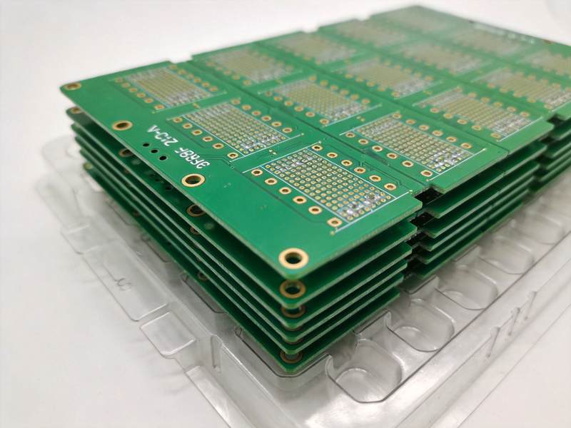
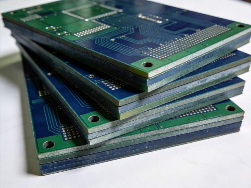
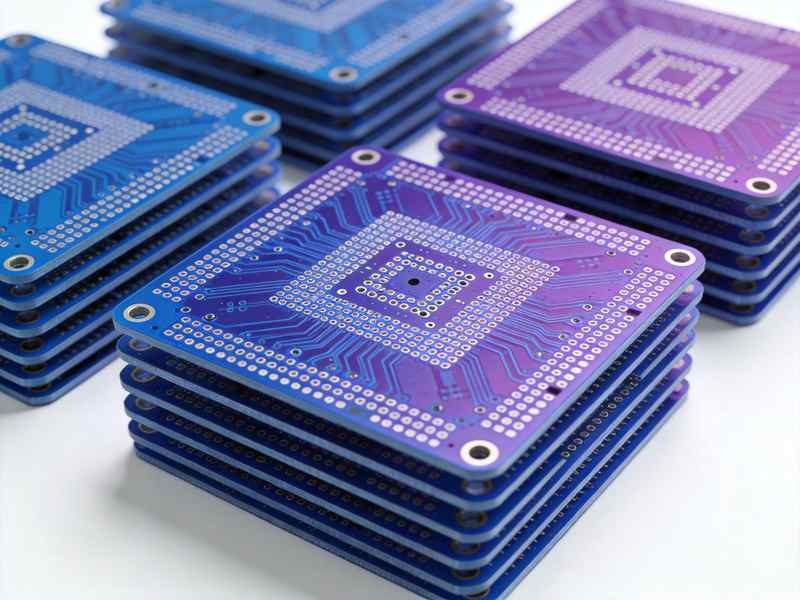
Standard FR-4 based rigid PCBs, the most widely used type in consumer electronics, industrial controls, and communication devices. Available from 1 to 32 layers with multiple surface finishes (HASL, ENIG, OSP, immersion silver/tin).

  • 1 - 32 layers
  • Min 3mil / 3mil trace & space
  • FR4 / High-Tg / Aluminum substrate
  • Lead time: 5 - 7 days for standard
Flexible PCB
02 / 08

Flexible PCB

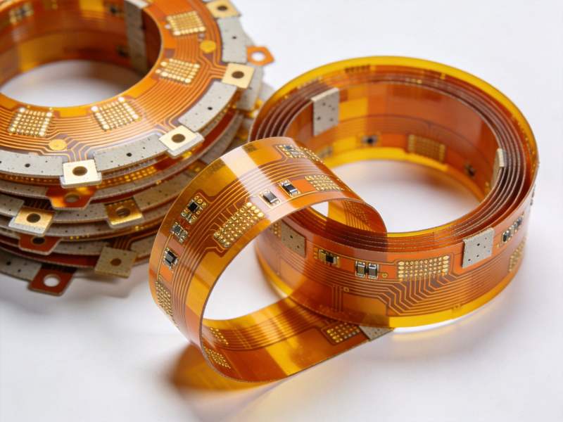
Polyimide-based flexible circuits that can bend, fold, and twist to fit tight spaces. Ideal for dynamic flexing applications and weight-sensitive designs — widely used in smartphones, wearables, cameras, and automotive sensors.

  • 1 - 8 flex layers
  • Thickness 0.05mm - 0.3mm
  • Polyimide / PET coverlay
  • Dynamic flex life ≥ 100,000 cycles
Rigid-Flex PCB
03 / 08

Rigid-Flex PCB

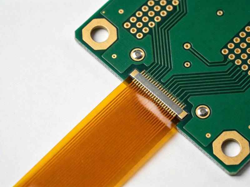
Combines rigid and flexible sections in a single board, eliminating connectors and cables while reducing assembly cost. Reliable under high vibration — the standard solution for aerospace, medical devices, military, and compact electronics.

  • 2 - 24 layers
  • FR4 rigid + Polyimide flex
  • Replaces connectors & cables
  • Lead time: 10 - 15 days
Rogers PCB
04 / 08

Rogers PCB

High-frequency laminates from Rogers Corporation featuring low dielectric loss (Df) and stable dielectric constant (Dk) for high-speed signal integrity. The go-to choice for RF, microwave, 5G base stations, radar, and satellite communications.

  • Rogers 4003C / 4350B / 5880
  • Dk 2.2 - 3.5 controlled
  • Low Df @ 10 GHz
  • 5G / Radar / Microwave
High Tg PCB
05 / 08

High Tg PCB

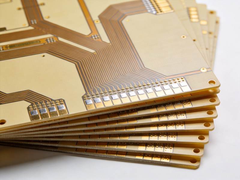
Tg (glass transition temperature) above 170°C, lead-free reflow capable and resistant to thermal stress during multiple reflow cycles. Designed for high-temperature environments and multilayer designs with heavy copper — automotive under-hood, industrial inverters, and power electronics.

  • Tg 170°C / 180°C
  • Lead-free reflow ≥ 6 cycles
  • Compatible with thick copper
  • Automotive / Industrial
High Frequency PCB
06 / 08

High Frequency PCB

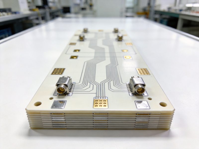
Engineered for high-frequency signal transmission with low loss and tight impedance control. Built on specialty substrates (PTFE, Taconic, RO4000 series) to maintain signal integrity at GHz frequencies. Used in 5G infrastructure, satellite, radar, and aerospace.

  • PTFE / Taconic / RO4350B
  • Impedance tolerance ±5%
  • Low Df for GHz signals
  • Telecom / Satellite / Radar
Heavy Copper PCB
07 / 08

Heavy Copper PCB

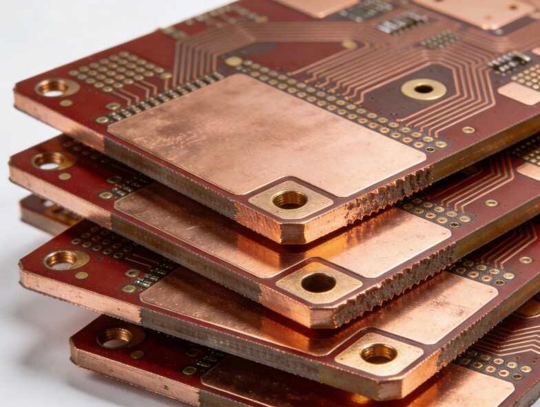
Copper thickness from 3oz up to 12oz per layer, capable of carrying high currents with excellent thermal management. The standard choice for power electronics, EV charging stations, industrial inverters, solar inverters, and high-power LED drivers.

  • 3oz - 12oz copper per layer
  • Current capacity 100A+ per trace
  • Plated copper up to 30oz
  • EV / Solar / Industrial Power
HDI PCB
08 / 08

HDI PCB

High Density Interconnect with laser-drilled micro vias, blind/buried vias, and fine 3mil/3mil line/space. Any-layer interconnection supports BGA, QFN, 0201 / 01005 component placement. The standard for smartphones, tablets, wearables, and 5G modules.

  • 1+N+1 / 2+N+2 / Any-layer stack-up
  • Laser micro via 0.075mm
  • 01005 / 0201 component capable
  • Lead time: 7 - 10 days

Service Advantages

  • Minimum trace width/spacing up to 3mil, meeting high-density interconnect requirements
  • Supports 1-32 layer board manufacturing, covering various application scenarios
  • Provides FR4, aluminum substrate, high-frequency board and other material options
  • Complete surface treatment processes: HASL, ENIG, OSP, immersion silver, etc.
  • Strict quality control system, ensuring the quality of every PCB

Technical Specifications

Layers 1-32 layers
Min Trace Width/Spacing 3mil/3mil
Min Hole Diameter 0.15mm
Max Size 600mm x 500mm
Board Thickness 0.2mm - 3.2mm
Copper Weight 0.5oz - 6oz

15 years of dedicating to PCB&PCBA manufacturing

Factory-direct • NDA Protected • 6h Response

Simply drop your email or phone number in the contact form, and we’ll promptly provide you with a quotation.

Get a Free PCB&PCBA Quote in 6 Hours

Up to 32-layer PCBs  | Precision SMT  |  ISO9001 & IATF16949 Certified